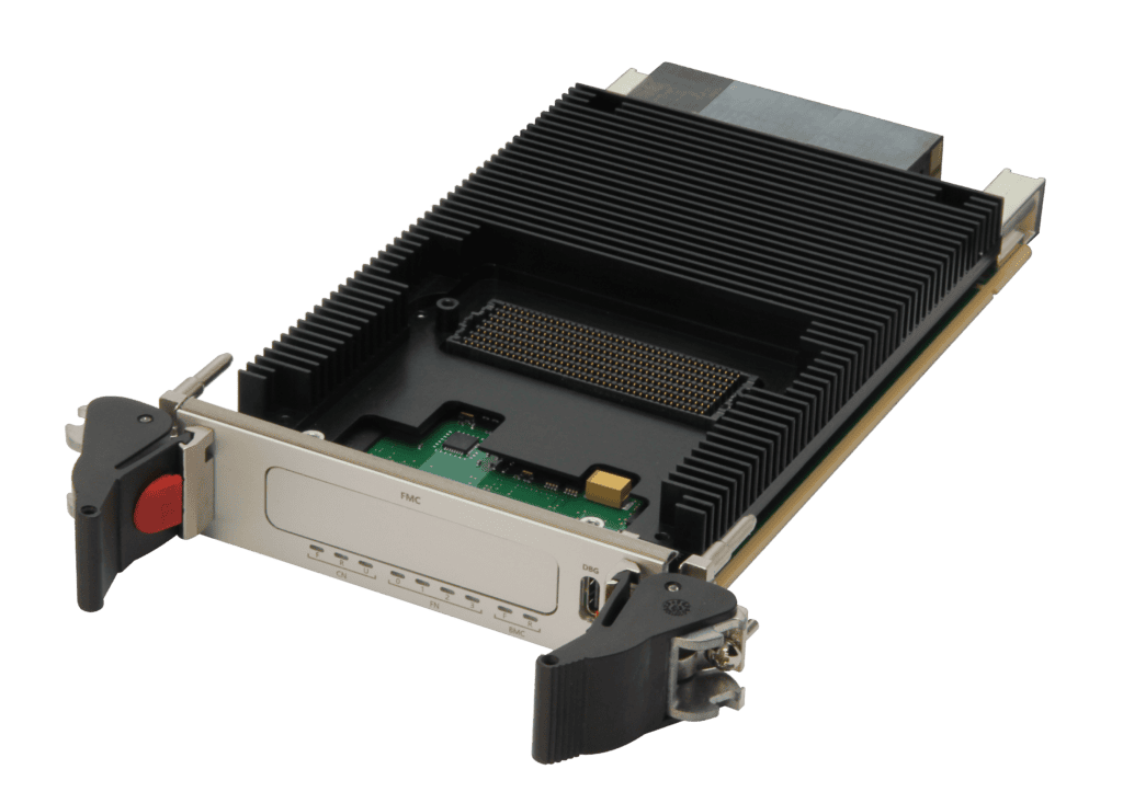
1 2 16

IC-ADDA-FMCPa

Dual 16-bit 28 GSPS DAC and Dual 12-bit 20 GSPS ADC

#9370db

Overview

The IC-ADDA-FMCPa can be plugged in the FMC site of the IC-FEP-VPX3h 3U VPX FPGA to make a high-perfomance 3U VPX bundle.
The IC-ADDA-FMCPa board is part of our Front End Processing product line to meet the increasing demand in fast data sampling for embedded systems especially in the field of Software-defined Radio, Radar and Electronic Warfare and solutions. The IC-ADDA-FMCPa is a VITA 57.4 FPGA Mezzanine Card (FMC) designed for applications requiring high data sampling. It offers a flexible connectivity with our 3U and 6U FPGA Front End Processing boards running our Signal Processing Example Designs (including signal acquisition, Processing DMA Engine, data storage, signal generation, etc) thus allowing customers to streamline development of high performance signal acquisition systems by concentrating their efforts on their most critical tasks.

Features

Analog Inputs
• Two ADCs channels with 12-bit resolution
• Sampling rate up to 20 Gsps
• SMPM connectors with lock feature
• Input impedance 50 Ohm AC coupled
• Full scale amplitude 500mV peak-peak (-2dBm)
• Analog input bandwidth (-3dB) 0.5GHz – 18GHz

Analog Outputs
• Two DACs channels with 16-bit resolution
• Sampling rate up to 28 Gsps
• SMPM connectors with lock feature
• Output impedance 50 Ohm AC coupled
• Full scale amplitude -2.6dBm for L nad, -3.5 dBm for X band
• Analog output bandwidth (-3dB) 2GHz – 18GHz

CLK/SYSREF Input
• SMPM connectors with lock feature
• Input impedance 50 Ohm AC coupled
• Input level. Sine wave: 0 to +10dB. Square wave
• Frequency range: CLK from 400 MHz to 800 MHz

FMC digital interface
• Electrical level CML
• 24 lanes
• Support 20Gbps for JESD204B, and up to 28.21 for JESD204C

Board Electrical/environmental features
• VITA 57.4 HPC single width module with Region 1 and
• front I/O
• Power dissipation: up to 40 W (TBC)
• FMC I/O voltage: 12V, 3.3V, VADJ = 1.5 V
• Air cooled and conduction cooled versions

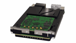
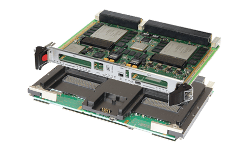
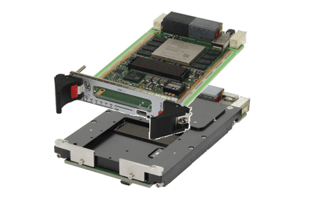
Bundle IC-FEP-VPX3h + IC-ADDA-FMCPa
Example of a bundle with the IC-FEP-VPX3h 3U VPX VITA 66.5 FPGA board with the plug-in IC-ADDA-FMCPa FMC module.

Diagram

IC-ADDA-FMCPa - diagram

Grades

StandardExtendedRuggedConduction-cooled 71°CConduction-cooled 85°C
CoatingOptionalYesYesYesYes
Operat. Temp.0 to 55°C-20 to 65°C-40°C to 71°C (*)-40°C to 71°C at the thermal interface (*)-40°C to 85°C at the thermal interface (*)
Rec. airflow1 .. 2 m/s2 .. 3 m/s2 .. 5 m/s--
Oper. HR% no cond.5 to 90%5 to 95%5 to 95%5 to 95%5 to 95%
Storage Temp.-45°C to 85°C-45°C to 85°C-45°C to 100°C-45°C to 100°C-45°C to 100°C
Sinusoidal Vibr2G [20..2000]Hz2G [20..2000]Hz5G [20..2000]Hz5G [20..2000]Hz5G [20..2000]Hz
Random Vibr0.002g2 /Hz [10..2000]Hz0.002g2 /Hz [10..2000]Hz0.05g2 /Hz [10..2000]Hz0.1g2 /Hz [10..2000]Hz0.1g2 /Hz [10..2000]Hz
Shock 1/2 Sin. 11ms20G20G40G40G40G

Related products

3U VPX VITA 66.5 FPGA board with FMC+ site
#d54444
  • 3U VPX – VITA 66.5
  • 1 * AMD Versal™ FPGA
  • 2 * DDR4 banks (up to 8GB each)
  • 1 * FMC+ site (VITA 57.4)
  • SLT3-PAY-1F1U1S1S1U1U2F1H-14.6.11
  • Aligned with the SOSA® Technical Standard
6U VPX FPGA board with two FMC+ sites
#d54444
  • 6U VPX
  • 2 * AMD Kintex™ UltraScale™/ Virtex™ UltraScale+™ FPGAs
  • 1 * NXP QorIQ LS1046A
  • Gen2/3 PCIe switch
  • Giga Ethernet L2 switch
  • 2 * FMC+ sites
3U VPX VITA 66.5 FPGA board with FMC+ Site
#d54444
  • 3U VPX – VITA 66.5
  • 1 * AMD Kintex™ UltraScale™ FPGA
  • 2 * DDR4 banks (up to 4GB each)
  • 1 * AMD Artix™7 control node
  • 1 * FMC+ site (VITA 57.4)

Thanks for your enquiry. Please contact our Sales Department for any further information about this product.