IC-ADC-FMCd
A/D 16-bit, Quad 310 Msps
Home > Products > IOs/Graphics/Storage/Serial > IC-ADC-FMCd
Home > Products > IOs/Graphics/Storage/Serial > IC-ADC-FMCd
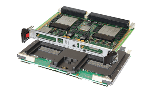
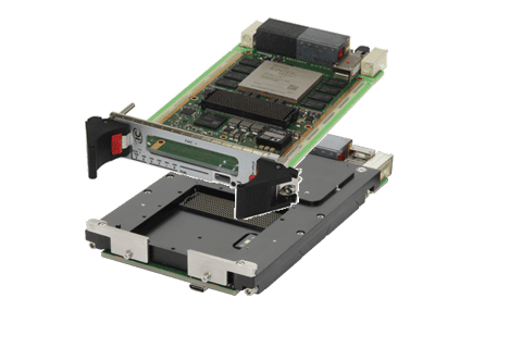
The IC-ADC-FMCd board is part of our Front End Processing product line to respond to the increasing demand in fast data sampling for embedded systems especially in the field of Software-defined Radio, Radar and Electronic Warfare solutions.
Designed for applications where high data sampling is required, the IC-ADC-FMCd is a VITA 57.1 FPGA Mezzanine Card (FMC).
It offers a flexible connectivity with our FPGA 3U and 6U Front End Processing boards running our Signal Processing Reference Design (including signal acquisition, Processing DMA Engine, data storage, signal generation,…) thus allowing customers to streamline development of high performance signal acquisition systems by concentrating their efforts on their most critical tasks. For new designs, we recommend you to use the IC-ADC-FMCPa.
Analog Inputs
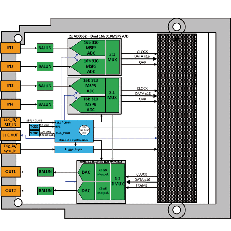
►Two AD9652 Analog Devices™ ADCs with 16 bit resolution
►Sampling rate from 80 to 310 MSPS
►4 channels with SSMC connectors
►Input impedance 50 Ω AC coupled
►Analog input bandwidth (-3dB) > 400 MHz. Full scale amplitude 2.5 V peak-peak
►SNR : 74 dBFS @Fin = 76 MHz, 72 dBFS @Fin = 173 MHz, 69 dBFS @Fin = 315 MHz, 66 dBFS @Fin = 400 MHz
►SFDR: 88 dBc @Fin = 76 MHz, 86 dBc @Fin = 173 MHz, 84 dBc @Fin = 315 MHz, 75 dBc @Fin = 400 MHz
►ENOB: 12.0 bit @Fin = 76 MHz, 11.6 bit @Fin = 173 MHz, 11.1 bit @Fin = 315 MHz, 10.8 bit @Fin = 400 MHz
Analog Outputs
►One AD9142A Analog Devices™ DAC with 16 bit resolution
►D/A update frequency : Up 1500M SPS with interpolation ratio x2, x4, x8
►Max sample rate:
►×2: 575 MSPS digital input / 1150 MSPS DAC update rate
►×4: 375 MSPS digital input / 1500 MSPS DAC update rate
►×8: 187.5 MSPS digital input / 1500 MSPS DAC up-date rate
►2 channels with SSMC connectors
►Output impedance 50 Ω AC coupled
►Analog bandwidth 500 MHz. Full scale amplitude 1 V peak-peak.
Clocks
►Sampling Clock (CKI) or Reference Clock (REFI):
►SSMC connector, 50 Ω , AC coupled
►Input level. Sine wave: 0 to +10dB. Square wave: LVPECL single ended
►Frequency range: >650 MHz
►Clock Output (CLK_OUT) :
►SSMC connector, 50 Ω , AC coupled
►0.8 V peak-peak
►300 MHz to 1600 MHz
►Clocking options (for both A/D and D/A clocks):
►External clock input (fanout buffer) 0.8 V peak-peak
►Synthesis through on-board VCO locked on either external reference (REFI), local 10 MHz TCXO or reference clock form carrier (FMC connector)
Trigger/Sync input
►SSMC connector DC coupled
►3.3 V logic input
►1.3 V threshold
ADC digital interface
►ADC Output : LVDS – 2 channels muxed on a 16-bit parallel bus. Data rate 620 Mbps per LVDS at 310 MSPS
►DAC Input: LVDS – 2 channels mixed on a 16-bit parallel bus. Up to 1150 Mbps per LVDS/ 575 MSPS per channel. Interpolation ratio x1, x2, x8
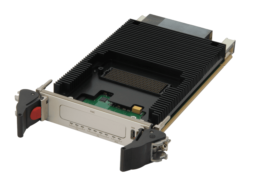
Board Electrical/environmental
►VITA 57.1 HPC single width module with Re-gion 1 and fron I/O
►Power dissipation: 8.5 W for Quad 16b 310 MSPS A/D model. 10 W for Quad 16b 310 MSPS A/D + Dual 16b 1500 D/A
►FMC I/O voltage: VADJ= 1.8 or 2.5V. 12P0V, 3P3V, 3P3V_AUX
►Air cooled, Rugged air cooled and conduction cooled
| Standard | Extended | Rugged | Air-Flow-Through | Conduction-cooled 71°C | Conduction-cooled 85°C | |
|---|---|---|---|---|---|---|
| Coating | Optional | Yes | Yes | Yes | Yes | Yes |
| Operat. Temp. | 0 to 55°C | -20 to 65°C | -40°C to 71°C (*) | -40°C to 85°C at the thermal interface (*) | -40°C to 71°C at the thermal interface (*) | -40°C to 85°C at the thermal interface (*) |
| Rec. airflow | (*) | (*) | (*) | (*) | - | - |
| Oper. HR% no cond. | 5 to 90% | 5 to 95% | 5 to 95% | 5 to 95% | 5 to 95% | 5 to 95% |
| Storage Temp. | -45°C to 85°C | -45°C to 85°C | -45°C to 100°C | -45°C to 100°C | -45°C to 100°C | -45°C to 100°C |
| Sinusoidal Vibr | 2G [20..2000]Hz | 2G [20..2000]Hz | 5G [20..2000]Hz | 5G [20..2000]Hz | 5G [20..2000]Hz | 5G [20..2000]Hz |
| Random Vibr | 0.002g2 /Hz [10..2000]Hz | 0.002g2 /Hz [10..2000]Hz | 0.05g2 /Hz [10..2000]Hz | 0.1g2 /Hz [10..2000]Hz | 0.1g2 /Hz [10..2000]Hz | 0.1g2 /Hz [10..2000]Hz |
| Shock 1/2 Sin. 11ms | 20G | 20G | 40G | 40G | 40G | 40G |
(*) Grades and conditions are subject to availability according to IC products. Please consult us or refer to user manuals.